Scientists Surpass Century-Old Limit on Converting Heat into Electricity


Scientists have reported a major breakthrough in thermoelectric materials after discovering a crystalline semiconductor capable of converting a temperature difference into an electrical voltage nearly 1,000 times larger than conventional textbook limits for solid materials.
The discovery, made by researchers from the Jawaharlal Nehru Centre for Advanced Scientific Research (JNCASR), the University of Sydney in Australia and the Indian Institute of Science (IISc), Bengaluru, challenges a long-standing assumption about how much electrical voltage can be generated from a temperature gradient in a crystalline solid.
The unusually large thermoelectric response could pave the way for a new generation of ultrasensitive temperature sensors, heat detectors, thermal imaging systems and quantum sensing technologies.
The researchers achieved the result using thin crystalline films of scandium nitride (ScN), a refractory transition-metal nitride. By carefully engineering the material’s electronic properties through controlled doping and charge compensation, the team produced thermoelectric voltages far beyond the range normally observed in conventional inorganic semiconductors.
Breaking a Long-Standing Thermoelectric Limit
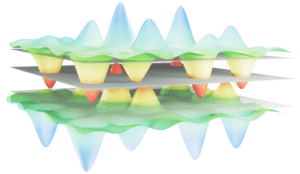
The phenomenon behind the discovery is known as the Seebeck effect. When two dissimilar materials or different regions of a material are maintained at different temperatures, mobile charge carriers move from the hotter region towards the colder region. This movement creates an electrical voltage.
The Seebeck effect, discovered nearly two centuries ago, forms the basis of technologies ranging from conventional temperature sensors to thermoelectric generators designed to convert waste heat into electricity.
The magnitude of this response is measured through the Seebeck coefficient, expressed in volts per kelvin. In most metals, the coefficient is only a few tens of microvolts per kelvin. Even high-performing semiconductor materials generally remain within the range of a few hundred microvolts per kelvin.
For decades, crystalline solids were thought to have a practical upper limit of only a few millivolts per kelvin.
Much larger values had generally been associated with liquid systems, including electrolytes, ionic gels and hydrogels, where ions rather than conventional electronic carriers play a major role in transporting charge.
The new research demonstrates that a fully crystalline semiconductor can move far beyond this presumed limit.
Engineered Scandium Nitride Shows Extraordinary Response
The research team was led by Prof. Bivas Saha of JNCASR, with Renuka Karanje, Dheemahi Rao, Diksha Dadhich and Sourav Rudra. The collaboration included Ashalatha Indiradevi Kamalasanan Pillai and Dr. Magnus Garbrecht from the University of Sydney and Prof. Subroto Mukerjee from IISc.
The researchers fabricated thin films of scandium nitride on magnesium oxide substrates using ultrahigh-vacuum magnetron sputtering.
ScN naturally contains free electrons associated with oxygen-related defects. To modify the electronic behaviour, the scientists deliberately introduced magnesium into the material. The magnesium doping was designed to compensate for the naturally occurring free electrons.
This created what researchers describe as a heavily doped, highly compensated (HDHC) semiconductor.
In such a material, positively and negatively charged dopant species are distributed throughout the crystal in nearly balanced proportions. The researchers found that this engineered disorder dramatically altered electronic transport and produced an exceptionally large thermoelectric response.
Importantly, structural examinations showed that the material retained its crystalline quality.
X-ray diffraction and atomic-resolution electron microscopy confirmed that the films remained single-crystalline and epitaxial, with the dopants distributed uniformly and without evidence of unwanted secondary phases or precipitates.
Seebeck Coefficient Far Beyond Conventional Semiconductors
The HDHC ScN films displayed a Seebeck coefficient several hundred to more than 1,000 times higher than typical values for inorganic semiconductors, according to the researchers.
The measured value exceeded –124.6 millivolts per kelvin near room temperature in a film approximately 200 nanometres thick.
That result is significant because it is far beyond the earlier range considered achievable in crystalline semiconductor systems and enters a regime more commonly associated with ionic and electrolyte-based materials.
The researchers describe the phenomenon as a solid-state equivalent of electrolyte-like thermopower, but occurring inside a fully crystalline semiconductor.
An additional surprise was that the effect became stronger as the ScN films were made thinner.
Prof. Bivas Saha said the researchers had not initially set out to break a thermoelectric record. The original objective was to understand how disorder and charge compensation affect electronic transport in scandium nitride.
The unexpected result, he said, demonstrated that engineered disorder could represent a largely unexplored route to achieving extreme thermoelectric and sensing performance in solid materials.
Prototype Photon Sensor Demonstrates Potential
To test whether the unusually large thermoelectric response could be translated into a practical device, the researchers developed a preliminary photon sensor.
The prototype used an HDHC ScN film with two chromium contacts. When a laser illuminated one of the contacts, it generated a small, localized temperature difference across the device.
That tiny temperature gradient produced a measurable electrical voltage. The resulting response corresponded to a Seebeck coefficient of approximately –102.4 millivolts per kelvin.
The researchers found that the voltage response was rapid and repeatable over multiple illumination cycles, with no apparent permanent change to the material.
The performance demonstrates that even a very small temperature difference can produce a comparatively large electrical signal.
The researchers believe that, with further optimisation, the technology could potentially be developed for extremely sensitive light detection, including applications approaching single-photon detection near room temperature.
An Indian patent application has also been filed covering thermoelectric thin-film materials and sensors for temperature and photon detection based on the research.
Potential Applications Across Sensing and Quantum Technologies
The unusually high thermoelectric response could have implications well beyond conventional heat-to-electricity conversion.
One of the most immediate possibilities is ultrasensitive temperature sensing. Because a small temperature difference can generate a relatively large voltage, devices based on the material could detect extremely small changes in temperature.
The technology could also contribute to low-noise thermal imaging, where detecting minute temperature variations is critical. Similarly, high-resolution heat-flux sensors could benefit from the ability to convert small thermal gradients into readily measurable electrical signals.
Other potential applications identified by the researchers include bolometric devices, which detect electromagnetic radiation through heating, and highly sensitive sensors for Internet-of-Things systems.
The material may also have applications in emerging quantum technologies. In particular, its strong thermoelectric response could potentially be exploited for cryogenic single-photon detectors, where detecting extremely weak optical signals is essential.
The researchers also observed a steep and well-defined temperature dependence of the thermoelectric response. This characteristic could potentially be used to develop temperature-controlled Seebeck switches, creating another possible route for future electronic and sensing devices.
A New Approach to Thermoelectric Materials
The findings suggest that the conventional approach to thermoelectric materials may need to be reconsidered.
Traditional research has often focused on improving thermoelectric performance by carefully controlling carrier concentration, crystal structure and other electronic properties while minimising unwanted disorder.
The ScN study points towards a different strategy: deliberately engineered disorder and charge compensation.
Rather than treating disorder only as something that degrades electronic performance, the researchers demonstrate that carefully controlled disorder can produce unusual electronic transport properties.
The work, published in the prestigious journal Science, therefore represents not simply a record for a particular material but a potentially broader design principle for solid-state thermoelectric technologies.
If the effect can be reproduced, controlled and integrated into practical devices, it could open a new class of highly sensitive thermal and photonic sensors.
The discovery demonstrates that a phenomenon traditionally associated with relatively modest voltages in crystalline solids can reach extraordinarily high levels when electronic structure, doping and disorder are engineered together. For technologies requiring the detection of tiny temperature changes or extremely weak light signals, that could provide a powerful new platform for sensing applications.