
India Unveils Semicon 2.0 to Expand Semiconductor Design, Manufacturing and Talent Ecosystem

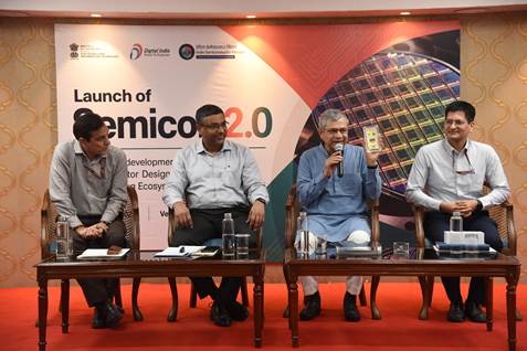
Union Minister for Electronics and Information Technology, Railways, and Information & Broadcasting Ashwini Vaishnaw on Monday outlined the government’s vision for taking India’s semiconductor ecosystem to the next level as notifications for all six pillars of the Semicon 2.0 Scheme were issued.
The new scheme builds on the momentum created by the first Semicon India Programme and seeks to strengthen India’s capabilities across the semiconductor value chain, including chip design, fabrication, assembly and packaging, equipment and materials, research and development, and talent development.
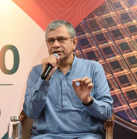
Addressing the media, Vaishnaw said India had achieved its earlier target of developing 85,000 semiconductor engineers in just four years, against a target originally set for 10 years. The government has now set a new target of developing one lakh additional semiconductor engineers, underlining the growing emphasis on building a skilled workforce for the industry.
Vaishnaw also said that India could account for close to 10 per cent of the global semiconductor industry’s market in the coming years, reflecting the government’s expectation of rapid expansion in domestic semiconductor manufacturing, design and related industries.
A key feature of the emerging ecosystem is the participation of students and institutions outside the country’s traditional technology hubs. According to Vaishnaw, students from Tier-II and Tier-III cities have already designed more than 250 semiconductor chips, indicating the widening reach of semiconductor education and design capabilities across India.
Six pillars of Semicon 2.0
The Semicon 2.0 Scheme will operate through six pillars covering 10 categories, providing fiscal and infrastructure support at different stages of the semiconductor value chain.
The first pillar focuses on semiconductor design. It covers the design of semiconductor intellectual property, chips, System-on-Chips (SoCs) and modules for national importance and strategic priorities. It will also support semiconductor IPs, chips and SoCs for the commercial sector, along with a Deployment-Linked Incentive for semiconductor IPs, chips and SoCs that reach deployment.
The second pillar focuses on machines and materials, with support aimed at strengthening the wider semiconductor manufacturing ecosystem. The availability of specialised equipment, machinery and materials is considered critical for developing a resilient domestic supply chain and reducing dependence on external sources.
The third pillar is aimed at setting up more semiconductor fabrication facilities, or fabs. It covers silicon semiconductor wafer fabs, compound semiconductor, photonics, sensors including MEMS, discrete semiconductor fabs, as well as display fabs.
The fourth pillar seeks to further strengthen the ATMP and OSAT industry. It will support semiconductor Assembly, Testing, Marking and Packaging (ATMP) and Outsourced Semiconductor Assembly and Test (OSAT) facilities, which form an important link between chip manufacturing and the final deployment of semiconductor products.
The fifth pillar focuses on research and development, particularly R&D related to advanced semiconductor technologies. The government intends to encourage innovation and help develop capabilities in emerging and sophisticated semiconductor technologies.
The sixth pillar is dedicated to talent development, with the objective of creating a larger pool of engineers, researchers, designers and other professionals required to support India’s expanding semiconductor industry.
Focus on supply-chain resilience and national security
The government has positioned Semicon 2.0 not only as an industrial policy but also as a strategic initiative linked to economic growth and national security.
Semiconductors are essential to a wide range of sectors, including telecommunications, automobiles, defence, consumer electronics, artificial intelligence, computing and industrial systems. The government aims to develop greater resilience across the semiconductor supply chain while strengthening India’s position as a technology and manufacturing hub.
The scheme is designed to provide support across the semiconductor value chain rather than concentrating exclusively on chip fabrication. This broader approach covers design, manufacturing, packaging, machinery, materials, research and human resources.
Vaishnaw highlighted the pace at which semiconductor projects are being developed in India. He said that in one instance, commercial production began just 13 months after the groundbreaking ceremony. He also pointed to faster regulatory clearances, noting that approvals had been granted within 200 days, 150 days and even 90 days in multiple cases.
The government expects the semiconductor ecosystem being developed under these initiatives to generate approximately 50,000–60,000 direct jobs, while also creating opportunities across associated industries and the wider technology supply chain.
Projects can run for up to six years
Projects supported under Semicon 2.0 will generally have a duration of up to six years. The scheme will initially remain open for applications for three years, providing companies and institutions with a defined window to seek government support.
The India Semiconductor Mission (ISM) will serve as the nodal agency responsible for implementing Semicon 2.0. ISM will invite applications, undertake technical and financial appraisal, recommend eligible applicants and oversee implementation of approved projects.
For certain design and deployment categories, ISM may work with the Centre for Development of Advanced Computing (C-DAC) to implement the programmes.
The India Semiconductor Mission may also introduce semiconductor deep-tech awards from 2026, aimed at encouraging niche innovation and supporting emerging technologies with potential strategic and commercial significance.
Mid-term assessment planned
The Ministry of Electronics and Information Technology will make budgetary provisions for providing fiscal support under the scheme. Disbursements will be made by the nodal agency in accordance with the approved conditions and eligibility requirements.
A mid-term assessment will be conducted after three years of implementation, or earlier if required. The assessment will examine the impact of the scheme and may consider modifications, continuation or other changes based on its performance.
The launch of all six pillars marks the next phase of India’s semiconductor strategy, moving beyond initial ecosystem creation towards a broader effort covering design, manufacturing, packaging, equipment, materials, research and skilled manpower.
With the government targeting another one lakh semiconductor engineers, expanding fabrication and packaging capacity, and encouraging chip design among students across Tier-II and Tier-III cities, Semicon 2.0 is intended to establish a more comprehensive domestic semiconductor ecosystem.
The government’s stated objective is to position India as a significant participant in the global semiconductor market while building greater technological self-reliance and supply-chain resilience. With expectations that India could account for nearly 10 per cent of the global semiconductor market in the coming years, the implementation of Semicon 2.0 is likely to play a central role in shaping the country’s semiconductor ambitions.